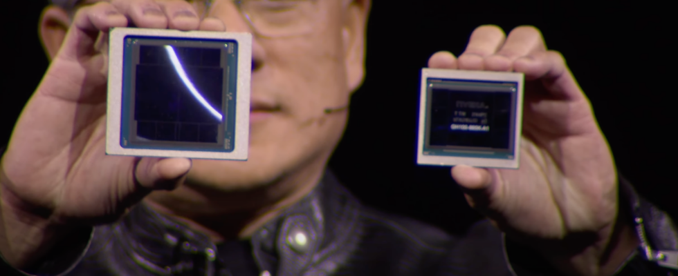
Jensen Huang, co-founder and CEO of Nvidia, showed off the new Blackwell chip, left, to compare it to its predecessor, H100, “Hopper.” Nvidia
Nvidia CEO Jensen Huang on Monday chaired the AI chipmaker’s first in-person technology conference since the COVID-19 pandemic, the GPU Technology Conference, or GTC, in San Jose, California, and revealed the company’s new design for its chips, codenamed “Blackwell.”
Many consider GTC to be the “Woodstock of AI” or the “Lalapalooza of AI.” “I hope you understand that this is not a concert,” Mr. Huang said following the loud applause that marked the start of the conference. He welcomed the list of partners and customers present.
“Michael Dell is sitting right there,” Huang said, noting that Dell’s founder and CEO was in the audience.
2,000 trillion floating point operations per second
Mr. Huang focused on the scale of computation needed to train the large language models of generative AI, or GenAI. A model with trillions of parameters, combined with training data representing trillions of “tokens”, or parts of words, would require “30 billion quadrillion floating point operations”, or 30 billion petaFLOPS, made notice Mr. Huang. “If you had a petaFLOP GPU, it would take you 30 billion seconds to calculate and train that model – 30 billion seconds is about 1,000 years.
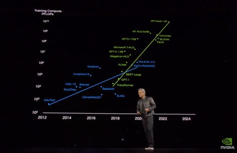
Mr. Huang began his presentation with an overview of the growing size of AI workloads, noting that the most powerful chips would take 30 billion seconds, or 1,000 years, to train. Nvidia
Nvidia’s H100 GPU, the newest chip, can perform around 2,000 trillion floating point operations per second, or 2,000 TFLOPS. A thousand TFLOPS equals one petaFLOP, meaning the H100 and its sibling, the H200, can only handle a few petaFLOPS, well short of the 30 billion Huang referenced.
“What we need is bigger GPUs – we need much, much bigger GPUs,” he said.
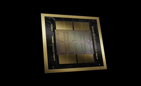
More than double the 80 billion transistors in Hopper GPUs
Blackwell, known in the industry as “HopperNext,” can achieve 20 petaFLOPS per GPU. It is intended to be delivered in an 8-way system, an “HGX” printed circuit board chips.
Using “quantization,” a kind of compressed mathematical operation where each value in a neural network is represented using fewer decimal places, called “FP4,” the chip can execute up to 144 petaFLOPs in an HGX system.
The chip has 208 billion transistors, Huang said, and uses a custom semiconductor manufacturing process from Taiwan Semiconductor Manufacturing, known as “4NP.” This is more than double the 80 billion transistors in Hopper GPUs.
The Nvidia Blackwell GPU increases the number of floating-point math operations per second tenfold and more than doubles the number of transistors of the “Hopper” series that preceded it. Nvidia highlights the chip’s ability to run large language models 25 times faster. Nvidia
AWS, Dell, Google, Meta, Microsoft, OpenAI, Oracle, Tesla and xAI among users
Blackwell can run large generative AI language models with a trillion parameters 25 times faster than previous chips, Huang said.
The chip is named after David Harold Blackwell, who Nvidia said was “a mathematician specializing in game theory and statistics, and the first black researcher inducted into the National Academy of Sciences.”
The Blackwell chip uses a new version of Nvidia’s high-speed network link, NVLink, which delivers 1.8 terabytes per second to each GPU. A discrete part of the chip is what Nvidia calls a “RAS engine”, to maintain the “reliability, availability and serviceability” of the chip. A set of decompression circuits improves the performance of things like database queries.
Early adopters of Blackwell include Amazon Web Services, Dell, Google, Meta, Microsoft, OpenAI, Oracle, Tesla and xAI.
GB200 Grace Blackwell Superchip
Like its predecessors, two Blackwell GPUs can be combined with one of Nvidia’s “Grace” microprocessors to produce a combined chip, called the “GB200 Grace Blackwell Superchip.”
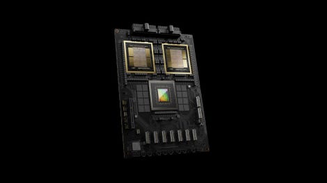
Like the Hopper GPUs that preceded it, two Blackwell GPUs can be combined with an Nvidia Grace microprocessor to produce a combined chip, called the “GB200 Grace Blackwell Superchip.” Nvidia
36 of the Grace and 72 of the GPUs can be combined for a rack computer that Nvidia calls the “GB200 NVL72” that can achieve 1,440 petaFLOPS, approaching the billion petaFLOPs cited by Huang.
A new system for the chips, the DGX SuperPOD, combines “tens of thousands” of Grace Blackwell Superchips, further increasing the number of operations per second.
Besides Blackwell, Nvidia made several other announcements:
- New generative AI algorithms to enhance its existing library of semiconductor design algorithms known as “cuLitho”, referring to photolithography used in the semiconductor design process. The GenAI code generates an initial “photomask” for lithography, which can then be refined by traditional methods.
It accelerates the design of these photomasks by 100%. TSMC and chip design software maker Synopsys are integrating cuLitho and new GenAI functions into their technologies. - A new line of network switches and network interface cards based on InfiniBand technology developed by Nvidia’s Mellanox, the “Quantum-X800 Infiniband”, and the Ethernet networking standard, the “Spectrum-X800 Ethernet”. Both technologies provide 800 billion bits per second, or 800 Gbps. Nvidia says the switches and network interface cards are “optimized for trillion-parameter GPU computing” to handle the speed of the chips’ floating-point operations.
- A catalog of 25 “micro-services” cloud-based application container services software, pre-built for individual applications, including custom AI models, built on top of the “NIM” container software suite from Nvidia, which in turn is part of the company’s AI Enterprise software offering.
The programs are what the company describes as a “standardized path to run custom AI models optimized for Nvidia’s CUDA installed base, which includes hundreds of millions of GPUs across clouds, data centers, workstations, and more. workstations and PCs”. Microservices include a set of life sciences-focused services, some of which are dedicated to “generative biology”, chemistry and “molecular prediction” tasks, to perform “inference”, generation of predictions, “for a growing collection of models in imaging, medical technology, drug discovery and digital health.” Microservices are available through systems from Dell and other vendors, through public cloud services including AWS, Google Cloud, Microsoft Azure, and Oracle Cloud Infrastructure, and can be tested on Nvidia’s own cloud service . - Earth-2, a separate microservice designed as a “digital twin” simulation of extreme weather, intended to “provide up-to-date alerts and forecasts in seconds, compared to minutes or hours in traditional CPU-driven modeling “. The technology is based on a generative AI model built by Nvidia called “CorrDiff”, which can generate “12.5 times higher resolution images” of weather models “than current digital models, 1,000 times faster and 3,000 times more energy efficient.” The Weather Company is an early adopter of this technology.
-
In addition to product and technology announcements, Nvidia announced a number of initiatives with partners:
- A collaboration with Oracle for “Sovereign AI” to run AI programs locally, “in the secure premises of a country or organization”.
- A new supercomputer for Amazon AWS built from DGX systems using Blackwell chips, called “Ceiba”.

You can watch the entire keynote speech on tape on YouTube.
Source: “ZDNet.com”