
The fineness of semiconductor engraving is a major issue for the three leaders in this sector of activity: TSMC, Samsung and Intel.
The awakening of Intel’s foundry activity is not only aimed at competing with the giant TSMC. Samsung is also in the crosshairs of the American company.
This is also felt by the South Korean group which has just made a notable change in the name of one of its most modern engraving processes… as if to show that it is not lagging behind?
From Intel 10nm to Intel 7
Until July 2021, the name of an engraving node was relatively self-explanatory and, regardless of the manufacturer, 22 nanometers was 22 nanometers and this did not seem to pose the slightest problem.
In July 2021, Intel decided to completely review the naming of its engraving nodes and to speak in “ equivalence “. This is how Intel’s 10nm changed its name to become the Intel 7. In the same way, the Intel 4 is a ” 4nm equivalent ”, but it is actually engraved in 7 nm. The reason for this change? A technological gap.
Intel had actually noticed that its 14 nm, but also its 10 nm are finer, more precise, in a word more advanced than those of the competition. In fact, on a chip engraved in 10 nm Intel, it would be possible to fit as many transistors as on a chip engraved in 7 nm TSMC.
Samsung renames SF3 to SF2
By renaming its engraving nodes, Intel therefore kills two birds with one stone. It keeps up with the technological level of its competitors while more directly reflecting the engraving quality of its own solutions.
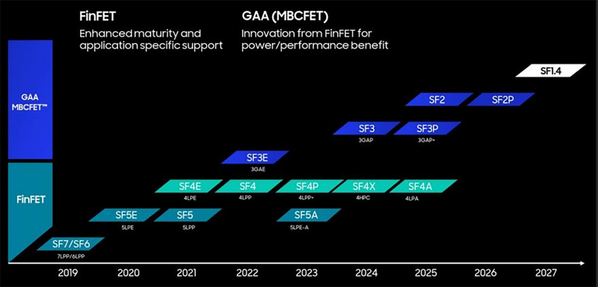
It seems that today a very similar movement is being made by the Samsung company. However, a more restricted movement which currently only concerns the SF3 engraving node. This second generation 3 nm process is now called SF2 in order, according to ZDNet Koreato position itself against Intel, which must deploy its “ 2nm equivalent » (Intel 20A) before the end of the year.
A change which is however not trivial insofar as it forced Samsung to revise all of the contracts signed around the SF3 in order to reflect the new name. Furthermore, Samsung does not give any technical reason for this change which is therefore only a marketing element: it is up to its customers to judge, as with Intel, the merits of this change in terminology which Samsung Foundry has yet to confirm.
Source : TechPowerUp, ZDNet
3