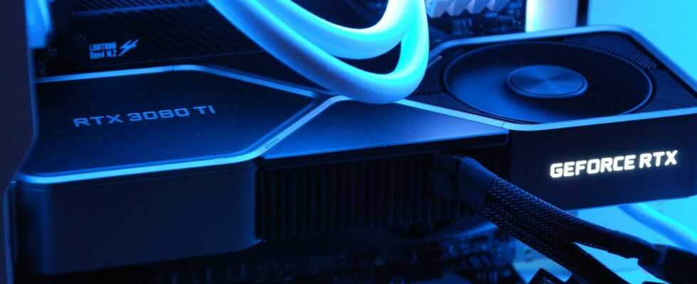
Victim of a cyberattack a few days ago, Nvidia is now subject to the publication of confidential data. These leaks concern in particular the GeForce RTX 40 and their Ada GPUs, some technical details of which have been revealed.
Previous rumors around the next generation of Nvidia graphics cards – which we can imagine will take the name GeForce RTX 40 – mentioned the use of the ADA architecture. Apart from this detail, which doesn’t tell us much about the capabilities of these graphics cards, we haven’t learned anything really concrete since except that this generation should mark a nice leap forward in terms of performance – still happy – and that the chip engraving will go through a 5 nm (TSMC) process against 8 nm (Samsung) for the GeForce RTX 30 GPUs.
This was without counting on the cyberattack suffered by Jensen Huang’s company at the end of February. The kidnappers threaten to reveal confidential details on the company’s projects and technologies if it does not deactivate the GeForce RTX 30’s LHR (Lite Hash Rate) mining limiter or if it does not make its graphics drivers free. Since then, data has been springing up everywhere. The DLSS source code has thus been unveiled and, even more interestingly, the first architectural details around the GeForce RTX 40s and their Ada GPUs.
Another Twitterian published ‘another AD102 block diagram’ first, but as the original creator, I will add a further explanation.https://t.co/7UoSeY3u30
Continued on next reply…—ftiwvoe (@ftiwvoe) March 2, 2022
The details revealed tell us that Nvidia should offer its own counterpart to AMD’s Infinity Cache. This would take the form of a large second-level (L2) cache, which would be shared by the GPU’s GPC blocks. This L2 cache would reach a maximum of 96 MB on the AD102 chip – high-end – which is much more than the maximum 6 MB of the GeForce RTX 30 under Ampere architecture. Obviously, the lower versions of the chips would not benefit from as much cache, the AD103 and AD104 GPUs would be limited to 64 MB when the entry-level AD106 and AD107 would be satisfied with respectively 48 MB and 32 MB.
Note: GAxxx GPUs correspond to GeForce RTX 30, ADxxx GPUs to RTX 40.
In addition, the transition to the fineness of engraving in 5 nm will make it possible to accommodate a much higher number of calculation units with an increase that can peak at 71% compared to the current generation of graphics cards. The AD102 chip would retain an area of more than 600 mm², as is already the case on the high-end GA102 chip of the GeForce RTX 3080 and above. It now remains to be seen whether the power consumption will not go to infinity and beyond… Recent rumors being not very encouraging on this subject, sometimes evoking more than 450 watts…