Picture: Samsung.
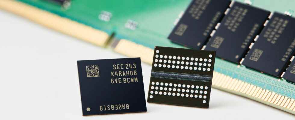
Samsung on Tuesday announced the development of a “double data rate 5” (DDR5) DRAM fabricated with a 12-nanometer (nm) process node.
According to the South Korean tech giant, the 12nm 16GB DDR5 DRAM has been verified with processor maker AMD, and its mass production is expected to start next year.
12nm
Samsung’s announcement is unusual, however. Indeed, when chipmakers announce a new chip, they usually refer to the process used to manufacture it as “10 nm class”, i.e. nodes with a size between 10 and 19 nm , or by their own jargon, without specifying the exact value. This time though, Samsung made it clear that the process node used was 12nm.
Samsung’s latest DRAM, to use its own term, is manufactured with its fifth-generation 10nm process node. If the Korean giant puts forward this numerical value of 12 nm, it is therefore probably to boast of its lead over its competitors in the 10 nm category.
However, it is difficult to know the actual size and density of transistors between chips made by different companies without testing, regardless of the names used to refer to them for marketing purposes, and they can differ significantly from each other.
Productivity increased by 20%
As for its 12nm 16GB DDR5 DRAM, Samsung says it used a new high-carbon material to increase capacitor volume and applied new designs to complement the new process node. Before adding that extreme ultraviolet (EUV) lithography was applied, to achieve the “highest density in the sector”.
These changes have increased productivity by 20% over the previous generation of DRAMs, meaning more can be made per wafer.
The chip boasts a maximum speed of 7.2 Gb/s, which means it can process 60 GB of data per second. Its energy consumption has been improved by 23% compared to the previous generation.
Samsung plans to launch other products in its 12nm DRAM lineup for applications in data centers, artificial intelligence and high-performance computing.
Source: ZDNet.com