No product has yet been announced, but the storage capacity of our SSDs should logically grow in large proportions.
Today, the most widely used 3D NAND – in SSD for example – is based on 96, 128 or even 176 layer chips. Techniques soon outdated by new products from Kioxia and Western Digital.
17 Gbit per square millimeter
Indeed, on the occasion of the Symposium on VLSI Technology and Circuits scheduled for June 11 to 16 in Kyoto, Japan, the two 3D NAND memory giants have planned some interesting announcements.
Of course, we will have time to come back to it when the presentations have been made, but in the meantime, the two companies could not resist the urge to make us languish. Thus, Kioxia is already talking about 3D NAND on 8 planes in 210 layers in order to reach impressive speeds of 3.2 GT/s.
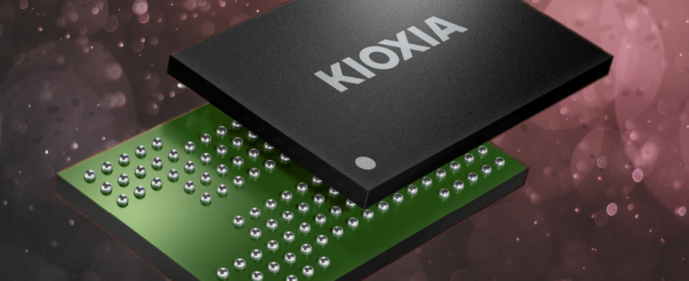
Kioxia here seems to present a variation of the integrated circuits already mentioned last March with Western Digital. This time it is a question of 1 Tbit modules capable of storing three bits per cell for a density of 17 Gbit per square millimeter.
Soon 3D NAND on more than 400 layers?
These integrated circuits with 210 layers on 8 planes are not, however, the only novelty mentioned by Kioxia, which has therefore once again joined forces with Western Digital to develop 3D NAND with more than 300 layers.
To do this, it is a question of a technique called “MILC” for Metal Induced Lateral Crystallization, which gives in very approximate French: lateral crystallization induced by metal. There, the two partners speak of 14-micron-long single-crystal silicon channels (“macaroni”). “Read noise” would be reduced by 40%, channel conductance increased tenfold, all without sacrificing cell reliability.
Finally, and this is the highlight of the show, there is talk of 3D NAND with more than 400 layers. There, we are talking about a new process developed by Tokyo Electron, which provides for ” quickly drill vertical channels over 10 microns “, to use the words of our colleagues from Tom’s Hardware. We don’t know much more for the moment, except the production of 3D NAND nodes with more than 400 layers by reducing the carbon footprint by 84% compared to the processes in use today.
Source : Tom’s Hardware
12