2
Samsung Electronics has just launched the mass production of semiconductors engraved in 3 nanometers. A key step for the South Korean giant, which trumps its great rival.
The mobility industry is the scene of a merciless battle between the various chip manufacturers. And every new breakthrough in engraving techniques is therefore closely scrutinized. Suffice to say that Samsung Electronics has just scored a serious point against its rival and world leader, the Taiwanese TSMC.
The South Korean giant has just announced the launch of mass production of semiconductors engraved on a 3 nm node. The FinFET architecture this time gives way to MBCFET, an in-house variant of GAA, for Gate-All-Around. The latter makes it possible to further reduce the size of the transistors without altering their ability to carry electric current.
Samsung has changed its burning process from the FinFET architecture. © Samsung Newsroom
Samsung Foundry obviously welcomed the news, stating that this manufacturing process was intended to be 45% more efficient in terms of energy consumption than that of 5 nm chips. It is also up to 23% more efficient, while the chips have seen their size reduced by 16%.
The firm has announced that it wants to further reduce consumption by 5% from the second generation of 3 nm chips, while offering 30% more performance. Suffice to say that the problems she had experienced with 4 nm engraving (on the Snapdragon 8 Gen 1 in particular) already seem to be ancient history.
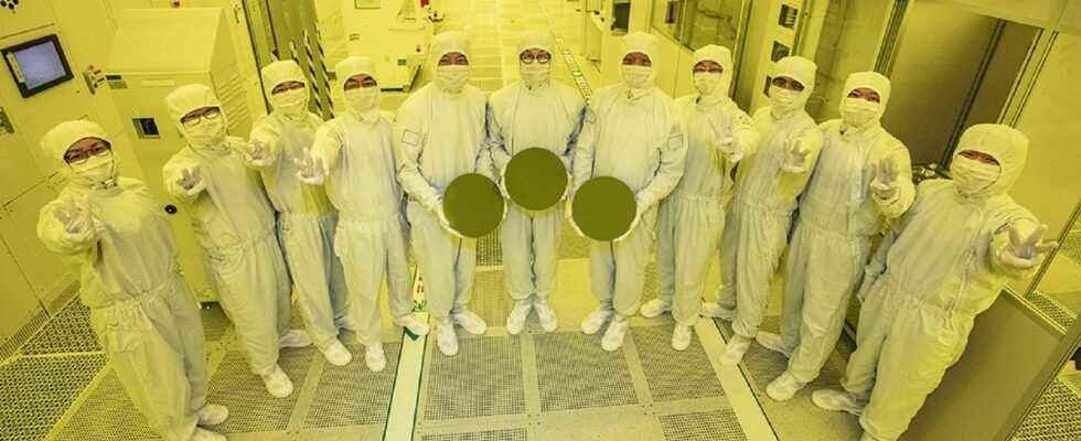
Samsung Foundry launches mass production of 3nm chips ahead of rival TSMC. © Samsung Newsroom
If TSMC is also to launch its 3 nm production this year, it should however keep the FinFET architecture. The transition to GAA would occur during the production of chips engraved in 2 nm. But the process is still in development, and should not see the light of day before 2026.
We imagine, however, that the news must have made noise in high places among the Taiwanese, who will have to jostle in the years to come to keep his throne.
Which SoC first?
If the new process is intended primarily for the computer market, mobile processors are obviously concerned. No official announcement has yet been made, but we can imagine that the American Qualcomm will use this new technique for its Snapdragon 8 Gen 2, which should be presented next November.
It is also possible that Samsung will reserve it for its next Exynos 2300. The opportunity to make people forget the semi-disappointment caused by the Exynos 2200, which fitted part of the Samsung Galaxy S22.