the GPUs
NVIDIA’s H100 will not be long in revealing itself in more detail and, above all, in an official manner.
Just this morning, we were talking about a final leak concerning Hopper, the new generation of GPUs designed by NVIDIA to equip data centers.
The opening of the GTC 2022 and the keynote presented by Jensen Huang, founder and CEO of NVIDIA, was an opportunity to clarify things.
TSMC N4 for 80 billion transistors
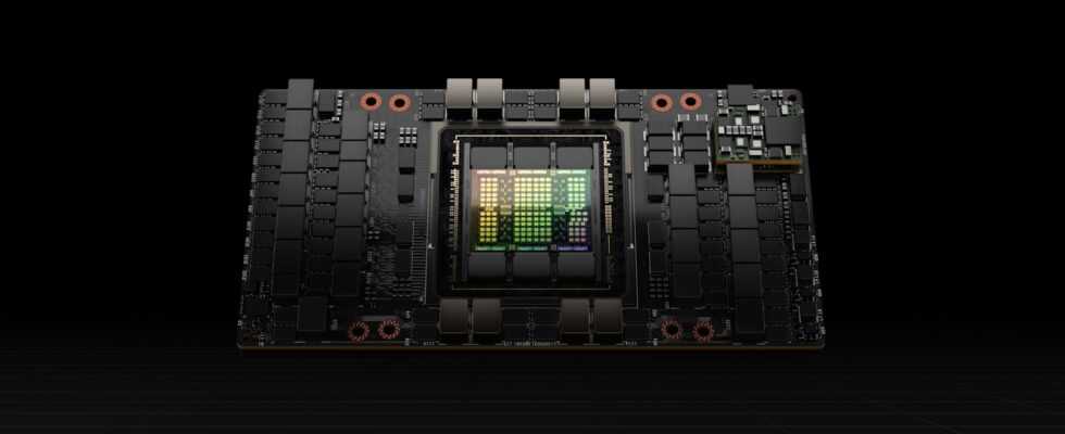
Contrary to what the rumors announced, this new GPU does not have 140 billion transistors, at least not for this Hopper generation H100 chip. NVIDIA has effectively indicated that it is a question of “only” 80 billion transistors.
The American, on the other hand, underlined the use of a very advanced engraving process since it is a question of the N4 from TSMC. Other great news, NVIDIA is using HBM3 memory on this generation: no less than 80 GB to be exact.
Two versions of the H100 having been mentioned by NVIDIA, the specifications vary. Thus, the H100 SXM displays an FP64 power of 30 teraFLOPS when the H100 PCIe has to be “satisfied” with 24 teraFLOPS. In fact, the TDP of the first is 700 W against 350 W for the second.
Finally, to complete the picture, NVIDIA talked about the integration of several H100 GPUs within the HGX H100 system: it integrates eight GPUs that communicate via fourth-generation NVLinks for maximum power.
Clubic independently and objectively compares the best models of graphics cards. Click for more information.
Read more
Source: NVIDIA
20