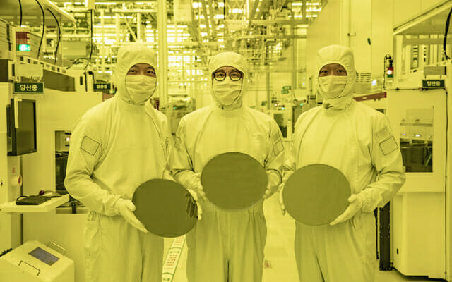
It’s a giant duel. South Korean company Samsung Electronics and Taiwanese company TSMC are racing to mass produce second-generation 3 nanometer (nm) processors this year. And it’s a long-distance race.
Because the parts manufactured this year will power products marketed in about two years. And they should succeed devices equipped with first-generation 3-nanometer chips. A generation whose marketing began in 2022.
According to Samsung Electronics, the second-generation 3-nanometer process uses a gate-all-around (GAA) process, with more efficiency compared to the first generation (SF3E). This performance is also 22% faster, with 34% higher power efficiency and 21% smaller logic area than Samsung’s previous 4-nanometer process.
Samsung has already reportedly secured a global server company as a customer of its second-generation 3-nanometer process.
TSMC for its part also plans to begin mass production of chips on the second-generation 3-nanometer process (N3E) during the first half of 2024 and on the advanced 3-nanometer process (N3P) during the second half of 2024. Mass production of the first generation 3 nanometer (N3) process began in December 2022.
According to TSMC, while the N3 process offered a 10-15% increase in performance and a 25-30% reduction in power consumption compared to the 5-nanometer (N5) process, the 3-nanometer (N3E) process of second generation ensures an 18% increase in performance and a 32% reduction in energy consumption. The N3P process offers a 5% increase in performance, a 5 to 10% reduction in power consumption and a 1.04 times increase in chip density compared to the N3E process.
TSMC’s customers for the second-generation 3-nanometer process include Apple, MediaTek, AMD, Nvidia and Qualcomm. Chips produced using the N3E process include the Apple A18 Pro, a mobile processor (AP) for the iPhone 16, which will be released in the second half of 2024.
FinFET vs. GAA
The 3 nanometer process stands out at both manufacturers in that Samsung has adopted a new generation transistor structure, known as GAA.
TSMC retained its existing process, FinFET (fine field-effect transistor).
Compared with the conventional Finfet structure, the GAA structure is considered to overcome transistor performance degradation due to miniaturization and increase data processing speed and energy efficiency. TSMC, for its part, plans to apply the GAA structure to its products using the 2 nanometer process.
“Thanks to Samsung’s early adoption of the GAA structure, the performance of the second generation of 3 nanometers has been more stable than that of the first generation,” says a source familiar with Samsung’s foundry business. “As advanced processes eventually move to GAA structures, Samsung could have an advantage because it acquired the know-how first.”
42 new foundries worldwide in 2024
On the production unit side, TSMC is investing massively in Japan, thanks to JASM, a joint venture with the Japanese companies Sony and Denso.
But global semiconductor production capacity will increase 6.4% year-on-year this year, to 31.5 million units. And the number of new factories is also expected to increase significantly around the world. The number of new semiconductor factories coming online this year is expected to reach 42, according to the Semiconductor Equipment and Materials Institute (SEMI).
The number of new semiconductor factories commissioned worldwide was 29 in 2022 and 11 last year.
“While investments contracted last year due to falling demand for semiconductors and inventory adjustments, this year we are seeing an upsurge in investments, driven by incentive policies in around the world,” SEMI said, “this trend will continue as the semiconductor supply chain becomes increasingly important to national and economic security.”
By country, China is the most active. Chinese semiconductor makers are expected to increase capacity by 13% year-on-year to 8.6 million parts per month, with 18 new lines coming online this year. For example, SMIC, the country’s largest foundry, will begin operations in new factories in Shanghai and Tianjin this year. The investment in these two factories alone amounts to $16 billion, but they will focus on mass production of 28-nanometer processes.
4nm in the United States
Taiwan, home to large foundries from TSMC and UMC (United Microelectronics Corporation), will also see five new fabs start up this year. Capacity is expected to reach 5.7 million units per month, an increase of 4.2% year-on-year.
In South Korea, capacity is expected to increase 5.4% year-on-year to 5.1 million wafers per month, as a new fab comes online. The new factory described in SEMI’s report is SK Hynix’s Cheongchu “M15X”, construction of which began in 2022, to produce 3D modules.
The United States is expected to see its capacity increase by 6% year-on-year to 3.1 million units per month, thanks to the commissioning of six new factories. Although this production appears minimal in volume compared to other countries, large companies such as Samsung Electronics, TSMC and Intel are investing in advanced processes in the United States.
Notably, Samsung Electronics will begin production of its 4-nanometer process at its new foundry plant in Taylor City in the second half of this year.
Towards 2nm and beyond
“If Samsung increases yields of its second-generation 3-nanometer process, it will have the opportunity to ‘fight back’ and challenge TSMC,” the source added.
Meanwhile, Samsung Electronics and TSMC aim to mass produce chips based on the 2-nanometer process starting next year.
Samsung plans to mass produce its 2-nanometer (SF2) process for mobile applications in 2025, then for high-performance computing (HPC) applications in 2026 and for automotive applications in 2027.
The 1.4 nanometer process is expected to be mass produced in 2027.
TSMC will introduce a 2-nanometer (N2) process next year and enhanced 2-nanometer processes N2P and N2X in 2026.
Intel has also entered the miniaturization bandwagon, planning volume production of its Intel Process 20A (2 nanometers) in the second half of this year and its Intel Process 18A (1.8 nanometers) next year.
Source: “ZDNet Korea”