The most modern engraving processes only concern three companies: Intel, Samsung and TSMC.
In recent months, Intel has monopolized a large part of the communication around semiconductor engraving processes. The American firm actually has the idea of getting back into the race.
But, of course, TSMC – the current number one in semiconductors – obviously does not intend to let itself be caught up without reacting. The latest roadmap from the Taiwanese group appears particularly ambitious.
Engraving at 1 nm in 2030
Organized a fortnight ago in San Francisco, the IEDM (International Electron Devices Meeting) was an opportunity for the main players to highlight some of their advances.
For TSMC, it was above all a question of dotting the “i”s and emphasizing how bright the future of the Taiwanese company is with a very ambitious roadmap which should make it possible to keep at bay its main competitors which are the American Intel and South Korean Samsung.
This roadmap is obviously not to be taken at face value insofar as TSMC can either get ahead or behind on what is therefore only a sort of forecast timetable to reach, current-2030 , the A10 engraving process.
More than a thousand billion transistors!
A process which will logically follow the A14 which must already evolve the N2/N2P by 2027. While the N2 is engraved in 2 nm, it is logically a question of 1.4 nm engraving for the A14 and engraving 1nm for the A10.
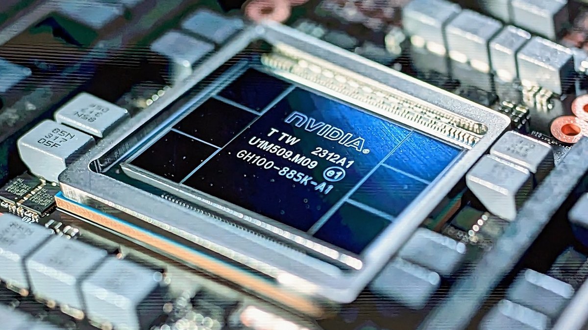
Such finesse will obviously not be without incredible technical challenges, but if TSMC is able to meet them, it should break records for transistor density. Currently, one of the most complex monolithic processors is NVIDIA’s GH100 with its 80 billion transistors, but TSMC is therefore planning to go much further.
Indeed, thanks to the A10 process, it would be possible to exceed 200 billion transistors on a monolithic chip by 2030. Of course, there is no question of only offering monolithic chips and TSMC does not forget advances in packaging that make it possible to create multi-chip chips as AMD and Intel can do.
Such advances have many names depending on their origin (CoWoS, InFO, SoIC, etc.) and TSMC estimates that thanks to these techniques, still by 2030, it will be possible to design chips embedding more than a thousand billion transistors. . A number that makes you dizzy.
Source : Tom’s Hardware
17