Last year we saw the first commercial use of chipsets manufactured using the 5nm process. For example, TSMC produced the first such chip found on a smartphone, the Apple A14 Bionic. The latter replaced the 7nm A13 Bionic chipset. The process node is based on the transistor density of a chip, which is the number of transistors that fit inside a square mm. This number is supposed to double every other year in theory, an observation called Moore’s Law first made by former Intel co-founder Gordon Moore in the mid 1960s and revised in the 1970s.
Apple might obtain access to 3nm chips well before other firms
For example, the A14 Bionic has a transistor density of 134 million transistors per square mm. That is 49% higher than the 89.97 million transistors per square mm used on the A13 Bionic. The 49% gain in transistor density resulted in a transistor count of 11.8 billion for the newer chip, up from the 8.5 billion transistors stuffed inside the A13 Bionic chipset. The reason why this is so important is that the higher the transistor density in a chip, the more powerful and energy-efficient that chip is. Both iOS and Android devices are benefiting this year from using 5nm chipsets. Besides the A14 Bionic, the Qualcomm Snapdragon 888 is a 5nm chip rolling off the assembly line at Samsung Foundry. And TSMC made the 5nm Kirin 9000 for Huawei’s HiSilicon unit before the U.S. blocked Huawei from receiving deliveries of its own chip.
FEATURED
VIDEO
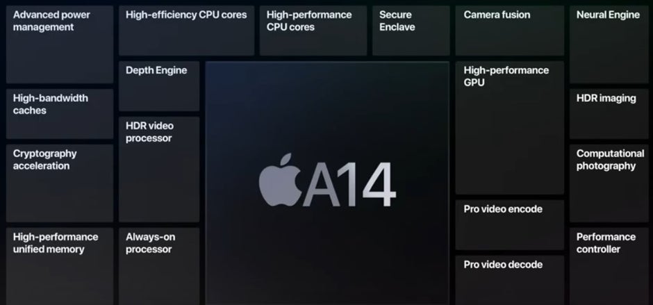
The A14 Bionic became the first 5nm chip ever used on a smartphone last year
Since Moore’s Law has yet to be repealed, both TSMC and Samsung Foundry have plans that take production down to 2nm with 3nm the next stop beginning later this year.
According to Sweclockers, TSMC could be starting Risk Production of its 3nm chips during the second half of this year. This would put TSMC a full year ahead of schedule as it battles with Samsung to remain the top contract foundry on the planet. While Samsung won back Qualcomm’s business for the 7nm Snapdragon 865 and the 5nm Snapdragon 888, a recent report says that TSMC will be the foundry of record for the 2022 Snapdragon chipset. That chip will reportedly be manufactured using TSMC’s 4nm process node.
Anandtech says that compared to the current top-of-the-line 5nm integrated circuits, 3nm chips will use 25%-30% less energy while delivering 10% to 15% higher performance at the same power levels. Transistor density will be up by 1.7x bringing that key number to approximately 227.8 million transistors per square mm. The TSMC foundry has the capacity to make 30,000 wafers per month for 3nm chips during 2021, rising to 105,000 by 2023-2024.
TSMC is expanding production of its wafers for 5nm chips with capacity rising to 105,000 each month during the first half of this year. That compares to the 90,000 wafers produced each month during the fourth quarter of last year. This will rise to 160,000 wafers produced each month starting in 2023-2024. The wafers for the generation-old 7nm chips are currently running off the line at a rate of 140,000 per month. This figure is expected to rise to 160,000 per month in two to three years.
The wafers for 3nm chips will be produced by TSMC later this year under “risk production.” This means that the wafers still might need some small changes before regular production begins. Apple is believed to have agreed to purchase all of the wafers that TSMC will churn out under risk production. While this will give Apple a head start in testing 3nm chipsets for the iPhone, it is very doubtful that the company would use these chips inside units of the iPhone 13 series destined for the hands of consumers. That is because in risk production, all of the risk will be on Apple, not TSMC. Chips from these wafers may not work right or might not work at all. Still, for Apple, spending money on wafers made during risk production is worth the, well, risk. It will give the tech giant access to faster and more energy-efficient chips before other firms.