
Nvidia revealed its next-generation AI GPU, named Blackwell, during its GTC 2024 keynote in San Jose, California.
Nvidia named its next-generation AI chip after David Harold Blackwell (1919–2010), a 20th-century American mathematician who established game theory, probability theory, information theory , etc.
“We need more powerful GPUs to learn and imitate text, images, graphs and even videos in languages around the world,” said Nvidia CEO Jensen Huang during his keynote speech.
Nvidia claims to have improved LLM processing speeds up to 30x
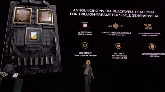
The Blackwell GPU is a chip made by connecting two semiconductor dies made using TSMC’s 4-nanometer process in Taiwan, with 208 billion transistors. The two dies operate as a single chip, exchanging 10 terabytes (TB) of data per second.
Built-in features include 5th generation NVLink, a connectivity pathway that can send and receive 1.8 TB of data per second back and forth between up to 576 GPUs, an AI-powered RAS engine that validates reliability of the GPU, and Secure AI which encrypts sensitive data and guarantees its authenticity.
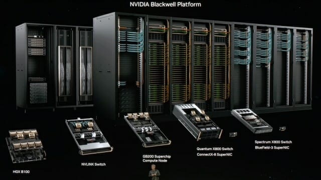
GB200 accelerator composed of two Blackwell GPUs and a Grace processor (Photo: nvidia)
The NVIDIA GB200 Grace Blackwell superchip
Going further, Nvidia introduced the NVIDIA GB200 Grace Blackwell superchip, which connects two NVIDIA B200 Tensor Core GPUs to the NVIDIA Grace CPU via a 900 GB/s NVLink chip-to-chip interconnect.
The GB200 is a key component of the NVIDIA GB200 NVL72, a multi-node, liquid-cooled rack system. It combines 36 Grace Blackwell Superchips, which include 72 Blackwell GPUs and 36 Grace CPUs interconnected by fifth-generation NVLink.
The GB200 NVL72 increases performance by 30x compared to the same number of NVIDIA H100 Tensor Core GPUs for LLM inference workloads, and reduces costs and power consumption by up to 25x.
The GB200 NVL72 is capable of 1.4 exaflops per second of AI computing and has 30TB of HBM3e memory. With this system, Nvidia claims to have improved LLM (large language model) processing speeds up to 30 times compared to a traditional 36 H100 system.
The HGX B200 accelerator
Nvidia is also launching the HGX B200, an accelerator that can use existing x86 processors such as Intel Xeon and AMD Epic. It includes eight TensorCore B200 GPUs and uses Nvidia’s Quantum2 Ethernet network to transfer data at speeds of up to 400 Gbps per second.
The Blackwell chip is expected to be available later this year. Major server vendors, including Cisco, Dell Technologies, HPE, Lenovo and Supermicro, will also offer Blackwell-based servers.
In addition to its own DGX cloud, Nvidia will offer Blackwell instances through major cloud providers around the world, including Amazon Web Services (AWS), Google Cloud and Microsoft Azure.
Source: “ZDNet Korea”