TSMC presented its plans for the near future. The arrival of the N3 process accompanied by the FinFlex technology is for the beginning of 2023, while the N2 is not expected before 2026 in our devices.
During its 2022 Symposium, TSMC unveiled its roadmap for its engraving processes detailing the N3 (3 nm equivalent), while paving the way for the N2 (2 nm equivalent) expected in 2025.
Increasingly long engraving processes
The N3 etching process is expected for the end of 2022 for availability in early 2023. It will be adopted by chip designers looking for the best available technology in order to take advantage of the advantages provided such as performance, power or surface area. engraving.
The N3 will be accompanied by the N3E, a process based on fewer layers, less efficient than the N3, but offering much better yields than the latter. The fact remains that the N3E offers 34% energy savings compared to the N5 at equal frequencies or 18% additional performance at equivalent consumption, all with a 60% higher transistor density. This engraving process is expected for mid-2023 with products available in early 2024.
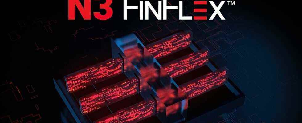
N3 FinFlex for more flexibility
With its N3 engraving process, TSMC will offer even greater customization thanks to FinFlex technology. Currently, with the N5 etching process, TSMC uses FinFet transistors with two ends. FinFlex makes it possible to mix the number of fins (fins) per transistor in order to obtain more or less efficient or more or less efficient blocks of transistors.
FinFlex makes it possible to offer 3-2 blocks for performance thanks to higher frequencies, more versatile 2-2 blocks with a balance between frequency and density, and particularly efficient 2-1 blocks with better efficiency and greater density, according to the founder.
The main advantage of the technology is that it is possible to mix the type of blocks according to the units on the same processor. This technology applied to a SoC will thus make it possible to burn high-performance CPU cores with 3-2 blocks, economical CPU cores in 2-2 and graphics units in 2-1 for example, it is up to the designer of the SoC to find the best compromise for its chip.
N2 in sight
TSMC also mentioned the arrival of the N2 process (2 nm equivalent), which will introduce GaaFet type transistors. The founder is already advancing on figures with 10 to 15% additional frequencies at equal power or 25 to 30% energy savings at equal speeds compared to the N3 process. The N2 process is scheduled for 2025.